Name of Business: Daltonium Isotopics
Relates to the substitution of isotopes of elements, instead of the mix of elements typically found in nature.
Nature of Business: Licensing manufacturing rights to patent invention isotope modification of dielectric used in Integrated Circuits.
https://www.freepatentsonline.com/y2021/0336027.html
Nature of Customers:
Integrated Circuit Manufacturers, primarily large and medium-sized manufacturers.
Probable List of Customers: Intel, Micron Technology, AMD, Broadcom, Qualcomm, TSMC, Samsung, Texas Instruments/National, Infineon (formerly International Rectifier), etc.
Nature of Market: These manufacturers build Integrated Circuits, which are physically small electronic components with (currently) up to 80 billion transistors on each.
Size of Market: Currently the market size is estimated at $630 billion worldwide.
Forecast to $1.91 trillion in 2032. See the yearly estimate:
https://www.precedenceresearch.com/integrated-circuit-market
Of this, probably 2/3s will be ICs that will depend on this technology.
Nature of product manufactured:
Integrated Circuits contain tiny components called "Transistors", or also called "MOSFETs", which stands for "Metal Oxide Semiconductor Field Effect Transistor".
The number of such MOSFETs which can be placed on a single device, or "die", has varied greatly over time:
| Year | Number of Transistors |
| 1970s | 10,000 |
| 1980s | 1 Million |
| 1990s | 100 Million |
| 2000s | 1 Billion |
| 2010s | 10 Billion |
| 2020s | 80 Billion |
What was the limitation to these products?
Primarily the limitation is the number of individual devices (MOSFETs) which can be placed on any given IC. This limits the complexity of the system which can be placed on that single chip.
This, in turn, is strongly related to the size of the smallest components, the individual MOSFETs themselves. (It is also related to the physical size of the silicon chip.)
A typical cutting-edge (best/smallest device manufactured) minimum feature size was 2,500 nanometers in 1980. As of 2007, a typical minimum feature size was 65 nanometers for the best manufacturers.
Today, the common best devices have a minimum feature size of 10 nanometer or 7 nanometer.
In 2007, the IC manufacturers had come to an impasse - they used an insulator, also called a "dielectric", made of silica (silicon dioxide; quartz) layer of silicon was created above a semiconductor channel, yet below the component called a "gate".
This dielectric had a figure of merit of 3.9, the so-called "dielectric constant". To obtain a minimum feature size of that era, 65 nanometers, they had to insulate the transistor gate with a thickness of 1.2 nanometers.
They could not make devices which had feature size smaller than 65 nanometer, because they could not create an insulator under a transistor gate thinner than 1.2 nanometer.
Why couldn't the transistor gate insulator get smaller/thinner than 1.2 nanometer?
1.2 nanometers is about 6x the thickness of a single silicon atom.
Silica consists of both silicon and oxygen atoms. It was necessary to consistently and reliably insulate possibly tens of billions of such transistors (MOSFETs) without error. Eventually, they could do this, HOWEVER, there was an additional problem.
The problem was a phenomenon called "Quantum Tunnelling" which caused a mysterious and unavoidable electrical current to flow between the gate and the semiconductor channel when the insulator thickness was smaller than 1.2 nanometer.
The insulator did not "break", the electrons simply jumped across the insulator, as if by magic. The size of this current was about 1 amp per square centimeter of IC area, which amounted to the wasting of a lot of power (as heat), and so was unacceptable.
The 'solution' was to keep the insulator thickness at 1.2 nanometer, or greater. But then, feature sizes of below 65 nanometers were not thought possible.
The entire IC industry would have been 'frozen' at that feature size. Fortunately, this problem had been anticipated, and help was on the way.
What recent breakthrough greatly improved this?
How did they get past the limitation of 65 nanometer feature size/insulation 1.2 nanometer limit?
During the early 2000's, scientists knew that this problem would eventually occur, and so they were looking for alternative insulators, other than silica/silicon-dioxide/quartz.
There were a handful of candidates. The best ones, they concluded, were compounds made of an element, "Hafnium".
For instance, hafnium oxide, with a dielectric constant of about 24, far greater than the 3.9 of silica/silicon dioxide - Ironically, this allowed the IC manufacturers to increase the thickness of the insulator to about 6 times of the 1.2 nanometers that previously limited them. This was approximately 7.2 nanometers, at least initially.
This meant that the "quantum tunnelling" leakage was no longer possible, at least at that stage. The industry could, and did, start making ICs with feature sizes less than 65 nanometers, and they did exactly this.
These are some early reports.
And about a year later:
But this reprieve, while it has lasted 15+ years, merely delayed the same problem, as the minimum feature size dropped again, the thickness of the insulators was fated to again approach that 'magic' 1.2 nanometer limitation.
Bad 'magic' - the problem? Scientists had already searched the Periodic Table, call it the 'grocery store' for elements, they had already chosen 'the best' solution, at least they thought so - what are they going to do?
Nature of invention - I'm the inventor, Jim Bell.
I have a BS degree in Chemistry from MIT, but also extensive knowledge in electronics, including some semiconductor physics.
From my chemistry education, I knew that elements in nature are sometimes, even usually, present in the form of multiple 'isotopes', which are commonly thought of as merely having different weights, caused by a different number of neutral particles, called "neutrons", in their nuclei
But if this difference was the only factor involved, there would have been no invention.
Keep in mind, first, that these isotopes are NOT RADIOACTIVE - they are stable, and exist forever.
But, I realized that there are additional differences between one kind of isotope and another.
I will focus now on Hafnium, which is present in six different isotopes.
https://www.webelements.com/hafnium/isotopes.html
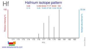
If the nucleus of an isotope has an odd number of neutrons, it has something called an "electromagnetic spin". You could think of it as an ultra-tiny 'bar magnetic' in space.
The two isotopes of hafnium which HAVE electromagnetic spin are: Hf-177 and Hf-179. The other isotopes of Hafnium do not.
When semiconductor manufacturers have used "Hafnium", from 2007 until and through today, they use the mix of isotopes which commonly exists in nature, which doesn't appreciably vary, they don't know how to do anything else.
They are not aware that there is any alternative - they don't realize that any improvement is even possible.
How do I plan to improve upon 'ordinary Hafnium' ?
What I believe is this - if these insulators are made either Hf-177, or Hf-179 (but, critically, not both), they will supply a much-greater dielectric constant, that key 'figure of merit' that scientists were chasing when they changed from using silica in 2007 to using Hafnium compounds that year
Is this possible? Yes! It turns out that there is a supply of such isotopes, both Hf-177 and Hf-179, having been separated in a device called a "Calutron", which amounts to a large 'mass spectrometer'.
https://www.webelements.com/hafnium/isotopes.html
And there are at least two sources, currently - the US Government, from a place called Oak Ridge, Tennessee, and a Russian company, JSC ISOTOP, in St Petersburg, Russia - and they can make more.
How much does this cost?
I got a quote a few years ago from JSC Isotope for each of those two 'interesting' isotopes - Hf-177 and Hf-179: Each was about $17,000 per gram
That sounds very expensive?
The good news is that to put a 2 nanometer thick layer on a 300 millimeter wafer (the current common size) takes 0.001 grams, or 1 milligram. Or $17 per wafer; reasonable.
But it gets better - the very large majority of this Hafnium compound is not needed everywhere on that wafer, and it will eventually be washed away, and so it can be recycled. I estimate 90% can be recycled, or more. So the actual amount needed will probably be less than $2 per wafer, after recycling - this is VERY reasonable!
How is this going to be prototyped?
To demonstrate the benefits of this invention, it will be necessary to prototype it, to demonstrate how well it works. To do that, I believe that a sample of about 3 grams of one of these isotopes (I expect to use Hf-179, for reasons I can explain) will be converted into the hafnium precursor, probably by a company called Millipore/Sigma/Aldrich, a well-respected chemical company that makes and sells tens of thousands of chemicals.
They already make hafnium precursors, using ordinary (non-isotope) hafnium. They install these chemicals into little cartridges that plug into vapor deposition machines.
There are other companies that work in this field - One is Applied Materials:
https://www.appliedmaterials.com/
Another company is Lam Research:
It will be necessary to measure the 'dielectric constant' of the as-deposited layer; this can be done by applying a layer of Hafnium compound, then covering that layer with an evaporated layer of metal, commonly aluminum. The capacitance across that layer will be measured electronically, and then the dielectric constant will be calculated, knowing the thickness of the layer and its area.
The plan:
1) Purchase a small quantity of Hf isotope, approx $17,000 per gram
2) Have that isotope converted into a precursor chemical, probably by Millipore/Sigma/Aldrich.
3) Design a test chip to test the dielectric constant of the new material
4) Pay a company to make a small test chip/part to test its cap/breakthrough voltage/etc
5) Send the chip/part out to an independent testing company to see the results and certify them
6) Publish the results to these companies and try to license the technique.
Some of these steps will typically be better accomplished by companies in that industry - they have the equipment and the expertise.
They will be very interested in helping to develop this new technology.
I would like to thank Mike Boyd for his assistance in creating this document.